The Journey to Hide a Nefarious WiFi Router in a Seemingly Normal USB Wall Charger
from hackster.io
A word about Pineapples
In the information/security world, WiFi Pineapples are specialized, purpose-built WiFi routers that were created by the team Hak5 for the express purpose of performing attacks, snooping on other devices, and sniffing sensitive data.
However, their form-factor makes them very easy to spot, which is what inspired Ryan Walker (who goes by Machinehum on Hackaday.io) to build a similar device that is housed entirely within a standard USB wall charger housing.
Overall, this special "WiFi Wart" project would run the ubiquitous openWRT OS on a custom PCB in order to cram it into such a small volume.
Required components
The microprocessor selected for this task was the Allwinner A33. Although it's older and not very fast, coming in at a blistering 1.2GHz on four cores, it is still powerful enough for this application.The chip also features many different kinds of peripherals including USB, I2C, SDIO (for connecting an SD card), PWM, and a real-time clock. Attached to this was 1GB of DDR3 RAM for the OS and networking stack. Finally, wireless connectivity is provided by a RealTek RTL8188CUS radio module.
Designing the hardware
Walker started his schematic by wiring together the DDR3 RAM module with the A33, which, thankfully, was quite easy to do. Next was the need for many different voltages, as each component requires one that's slightly below the standard 3.3v that most microcontrollers take.To do this, Walker chose the TPS62095RGTR switch-mode regulator for its efficiency and soft start pin. You can view the schematic in more detail here on GitHub.
For the board design, Walker went with a four-layer board since the routing would be quite dense in order to maximize space. The DDR3L SDRAM IC in its 96-bin ball-grid-array package was placed to the top-right of the A33.
Its routing to the microprocessor needed some extra consideration since the clock pins had to be within 0.2mm in length and the two halves of the data pins each had to be within 1.27mm of each other to ensure signal integrity. After doing some preliminary routing, KiCad was able to automatically add copper "squiggles" at certain points to extend the lengths to match.
Once the power management circuit had been added, the design was sent off for fabrication.
PCB troubles
Walker was able to assemble his newly-minted PCBs by placing a layer of solder paste on each pad via a stencil and then baking them in a reflow oven.When it came time to test the voltage output of the 2.5V regulator, it was discovered that it was outputting 3.3V instead and overloading the A33's peripherals. But after ordering the correct part this problem was rectified.
The next impasse came when Walker was trying to decide how best to integrate the power delivery system, whose job it is to take 120VAC from the wall and convert it into suitable voltages for the onboard components and USB ports.
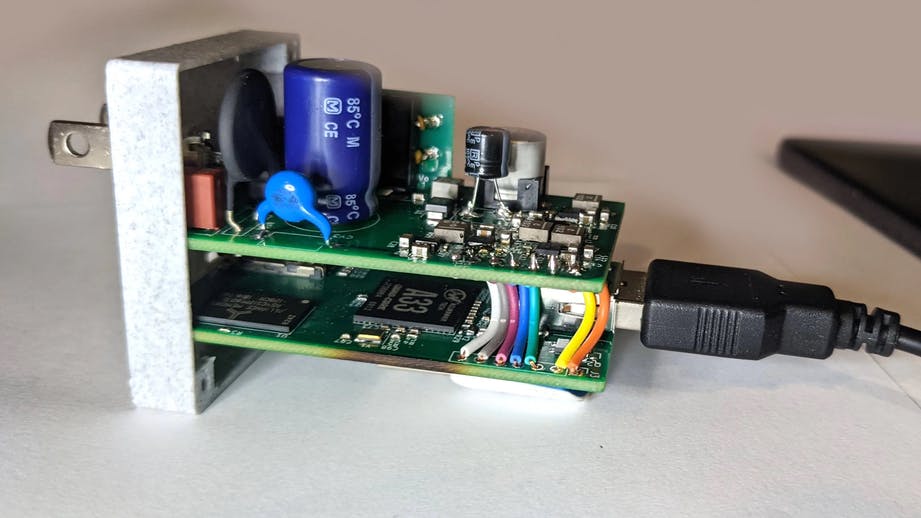
Because of the need for added safety and RF noise isolation, Walker went with the two-board solution. This second board houses a PBO-15C-5 module from CUI that takes the high-voltage mains power and converts it to 5V DC at up to 2.8A. This power board simply stacks on top of the main board and delivers power over a 0.1" header.
Loading the firmware and doing some quick tests
With the hardware side of things figured out, Walker refocused his sights on the firmware. For this task, he used Buildroot to load the bootloader, kernel, OS, and applications from an SD card onto his device, which in this case is the A33-OLinuxXino since it is quite similar to the hardware on the custom PCB.
Once it booted, Walker loaded all of the typical networking applications he could think of, along with the driver for his WiFi module. After connecting to his home's WiFi network, his WiFi Wart project was finally ready.
Assembly and future plans
Walker was able to design and 3D print a plausible-looking wall charger housing for his project that could contain both PCBs. And although he ran into some issues related to the worldwide chip shortage, he was eventually able to get everything he needed for a final prototype.
In its current state, the WiFi Wart boots up from an SD card and loads/runs all of its networking tools that can snoop on wireless packets, perform attacks, and much more. For more details about this six-month project, you can visit its Hackaday.io page here.


Leave a comment